User Tools
This is an old revision of the document!
System Plots
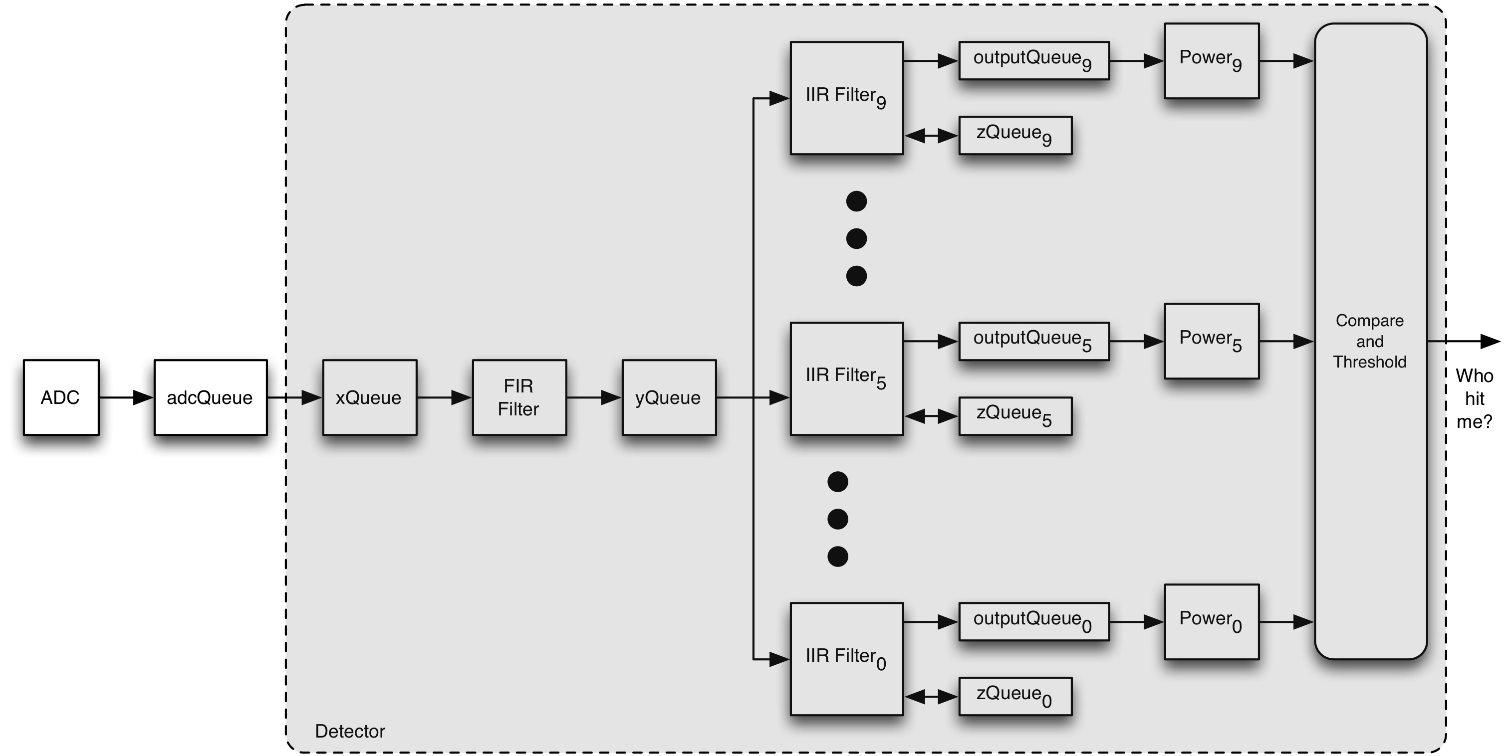
This is basic block diagram of the system.
The basic process is the following:
- Read numbers from the receiver board using the ADC at a rate of FS=100 kHz
- Low pass filter the samples (using an FIR filter)
- Down sample the data to a rate of FS=10 kHz
- Filter the data through the 10 bandpass filters (using 10 IIR filters)
- Compute a running power
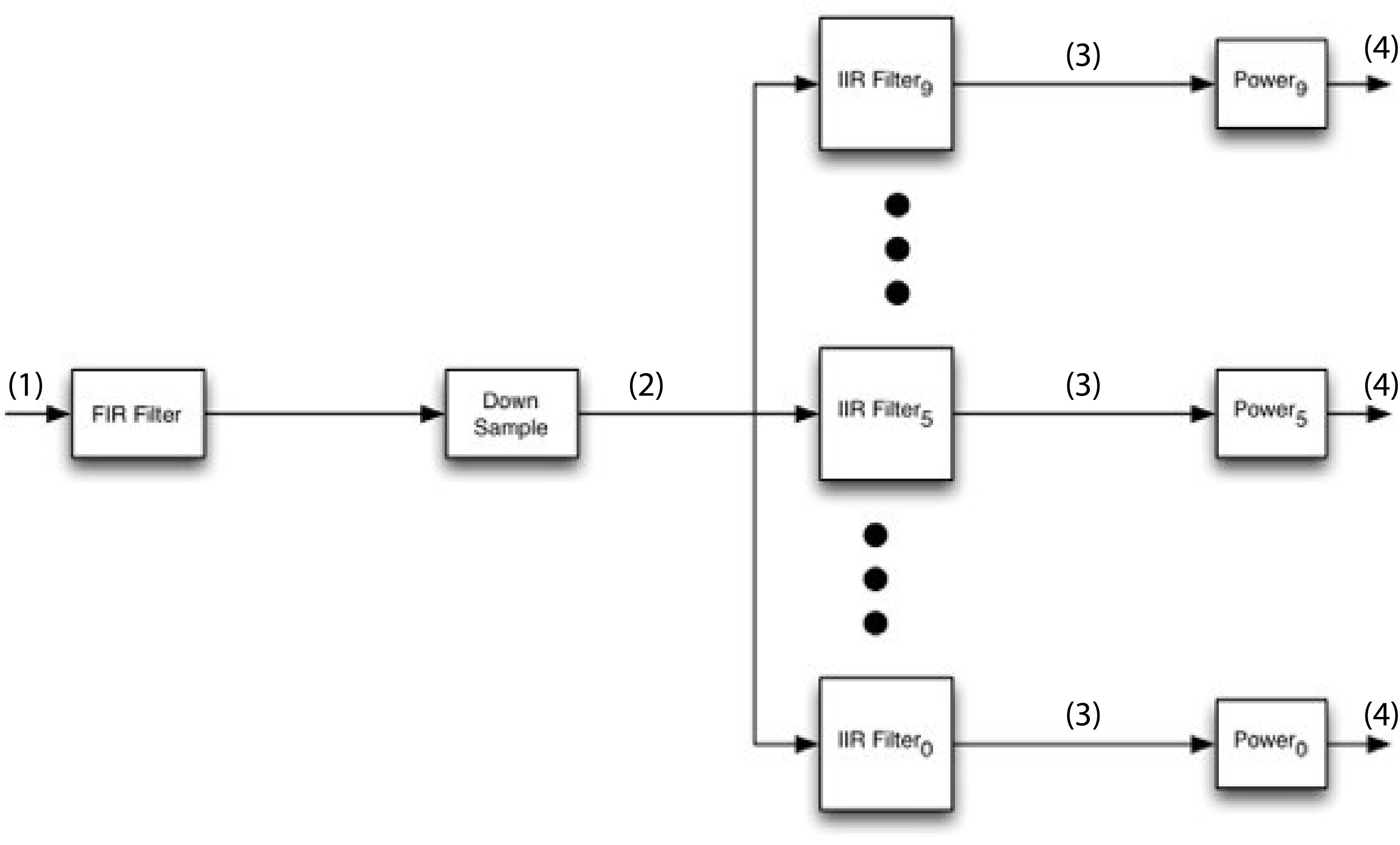
To better understand this process let's look at what the data would look like at various points in the design. The following block diagram is a simplified version of the previous block diagram. In this block diagram the queues have been removed since those are related to the way that the data structures are implemented.
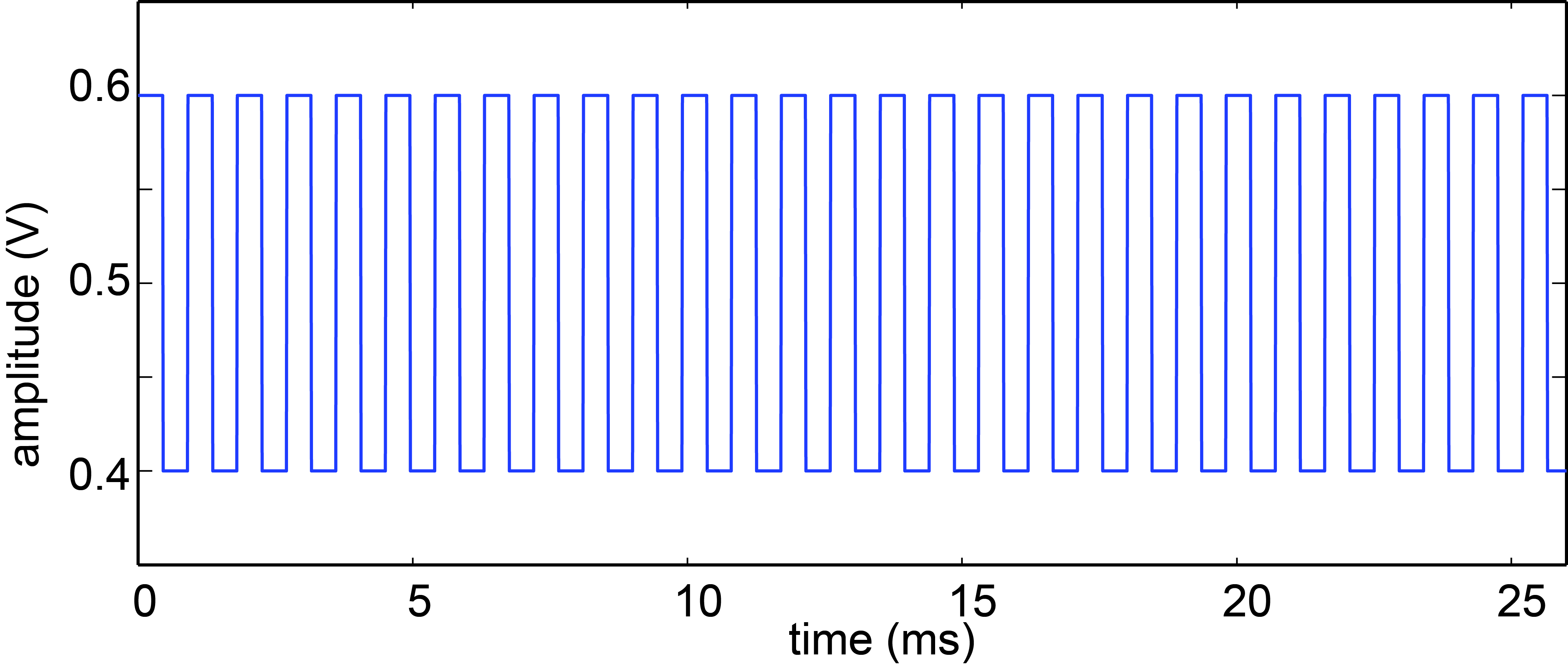
We are going to start by looking at a signal that is a square wave without any noise. This initial plot is at location (1) on the block diagram. This signal is a square wave with frequency of f=1111 Hz, amplitude of 0.2 V peak-to-peak, and has an offset voltage of 0.5 V. We have zoomed in on the first 25 ms of time so that it is easy to see the square wave oscillations
Low pass filtering We are going to start by looking at a very short time scale in order to easily see what things look like a t


